Quantum Chips Enter Industrial Manufacturing
How the SUPREME Pilot Line Is Bridging Research and Scalable Production Made in Europe

Multi-project superconducting qubit structures wafer
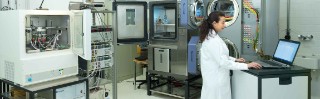
In the EU research project SUPREME, 23 partners from 8 member states are pooling their expertise to advance the development of stable manufacturing processes for superconducting quantum chips. The R&D activities specifically address the challenges related to the stability and yield of qubits – crucial factors for the scaling of quantum technologies and thus for Europe’s competitiveness in the global quantum hardware market.
more info